- 您现在的位置:买卖IC网 > Sheet目录312 > AT26DF081A-SSU (Atmel)IC FLASH 8MBIT 70MHZ 8SOIC
�� �
�
�10.2�
�Write� Status� Register�
�The� Write� Status� Register� command� is� used� to� modify� the� SPRL� bit� of� the� Status� Register�
�and/or� to� perform� a� Global� Protect� or� Global� Unprotect� operation.� Before� the� Write� Status� Regis-�
�ter� command� can� be� issued,� the� Write� Enable� command� must� have� been� previously� issued� to�
�set� the� WEL� bit� in� the� Status� Register� to� a� logical� “1”.�
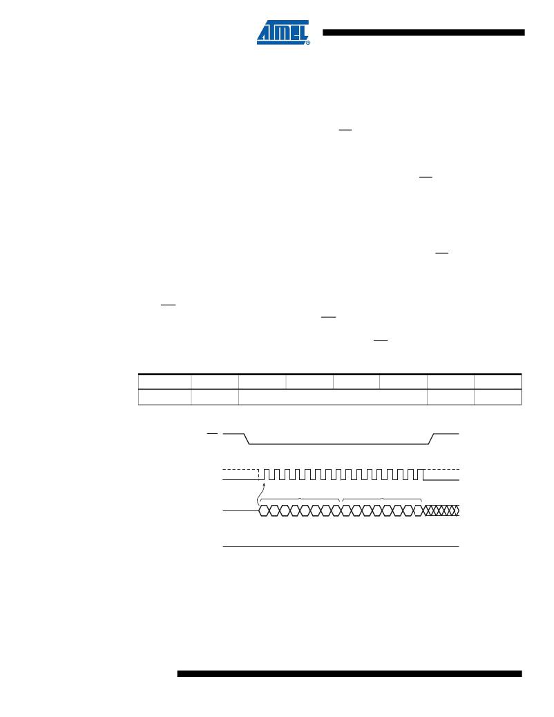
�To� issue� the� Write� Status� Register� command,� the� CS� pin� must� first� be� asserted� and� the� opcode�
�of� 01h� must� be� clocked� into� the� device� followed� by� one� byte� of� data.� The� one� byte� of� data� con-�
�sists� of� the� SPRL� bit� value,� a� don’t� care� bit,� four� data� bits� to� denote� whether� a� Global� Protect� or�
�Unprotect� should� be� performed,� and� two� additional� don’t� care� bits� (see� Table� 10-2� ).� Any� addi-�
�tional� data� bytes� that� are� sent� to� the� device� will� be� ignored.� When� the� CS� pin� is� deasserted,� the�
�SPRL� bit� in� the� Status� Register� will� be� modified,� and� the� WEL� bit� in� the� Status� Register� will� be�
�reset� back� to� a� logical� “0”.� The� values� of� bits� 5,� 4,� 3,� and� 2� and� the� state� of� the� SPRL� bit� before�
�the� Write� Status� Register� command� was� executed� (the� prior� state� of� the� SPRL� bit)� will� determine�
�whether� or� not� a� Global� Protect� or� Global� Unprotect� will� be� performed.� Please� refer� to� the�
�“Global� Protect/Unprotect”� section� on� page� 18� for� more� details.�
�The� complete� one� byte� of� data� must� be� clocked� into� the� device� before� the� CS� pin� is� deasserted;�
�otherwise,� the� device� will� abort� the� operation,� the� state� of� the� SPRL� bit� will� not� change,� no�
�potential� Global� Protect� or� Unprotect� will� be� performed,� and� the� WEL� bit� in� the� Status� Register�
�will� be� reset� back� to� the� logical� “0”� state.�
�If� the� WP� pin� is� asserted,� then� the� SPRL� bit� can� only� be� set� to� a� logical� “1”.� If� an� attempt� is� made�
�to� reset� the� SPRL� bit� to� a� logical� “0”� while� the� WP� pin� is� asserted,� then� the� Write� Status� Register�
�command� will� be� ignored,� and� the� WEL� bit� in� the� Status� Register� will� be� reset� back� to� the� logical�
�“0”� state.� In� order� to� reset� the� SPRL� bit� to� a� logical� “0”,� the� WP� pin� must� be� deasserted.�
�Table� 10-2.�
�Write� Status� Register� Format�
�Bit� 7�
�Bit� 6�
�Bit� 5�
�Bit� 4�
�Bit� 3�
�Bit� 2�
�Bit� 1�
�Bit� 0�
�SPRL�
�X�
�Global� Protect/Unprotect�
�X�
�X�
�Figure� 10-2.� Write� Status� Register�
�CS�
�0�
�1�
�2�
�3�
�4�
�5�
�6�
�7�
�8�
�9�
�10� 11� 12� 13� 14� 15�
�SCK�
�OPCODE�
�STATUS� REGISTER� IN�
�SI�
�0�
�0�
�0�
�0�
�0�
�0�
�0�
�1�
�D�
�X�
�D�
�D�
�D�
�D�
�X�
�X�
�MSB�
�MSB�
�SO�
�HIGH-IMPEDANCE�
�26�
�AT26DF081A�
�3600G–DFLASH–06/09�
�发布紧急采购,3分钟左右您将得到回复。
相关PDF资料
AT26DF161-SU
IC FLASH 16MBIT 66MHZ 8SOIC
AT26DF161A-MU
IC FLASH 16MBIT 70MHZ 8QFN
AT26DF321-SU
IC FLASH 32MBIT 66MHZ 8SOIC
AT27BV010-90JU
IC OTP 1MBIT 90NS 32PLCC
AT27BV020-90JU
IC OTP 2MBIT 90NS 32PLCC
AT27BV040-12JU
IC OTP 4MBIT 120NS 32PLCC
AT27BV1024-90JU
IC OTP 1MBIT 90NS 44PLCC
AT27BV256-70JU
IC OTP 256KBIT 70NS 32PLCC
相关代理商/技术参数
AT26DF081A-SSU-RET
制造商:Atmel Corporation 功能描述:
AT26DF081A-ST-B
制造商:Adesto Technologies Corporation 功能描述:8-SOIC-W, AUTO GRADE 3, 2.7V, TUBE - Rail/Tube
AT26DF081A-ST-T
制造商:Adesto Technologies Corporation 功能描述:8-SOIC-W, AUTO GRADE 3, 2.7V, T&R - Tape and Reel
AT26DF081A-SU
功能描述:闪存 8M 8 I/O Pins SPI 256B 2.7V-3.6V RoHS:否 制造商:ON Semiconductor 数据总线宽度:1 bit 存储类型:Flash 存储容量:2 MB 结构:256 K x 8 定时类型: 接口类型:SPI 访问时间: 电源电压-最大:3.6 V 电源电压-最小:2.3 V 最大工作电流:15 mA 工作温度:- 40 C to + 85 C 安装风格:SMD/SMT 封装 / 箱体: 封装:Reel
AT26DF081-MU
制造商:Adesto Technologies Corporation 功能描述:SF DATAFLASH, 8M, MLF, IND TEMP,GREEN - Trays
AT26DF081-SU
制造商:Adesto Technologies Corporation 功能描述:SF DATAFLASH, 8M, SOIC ,IND TEMP, GREEN - Rail/Tube
AT26DF161
制造商:ATMEL 制造商全称:ATMEL Corporation 功能描述:16-megabit 2.7-volt Only Serial Firmware DataFlash Memory
AT26DF161_06
制造商:ATMEL 制造商全称:ATMEL Corporation 功能描述:16-megabit 2.7-volt Only Serial Firmware DataFlash Memory